| Index | wersja polska |
Vague description of the NUM pin quoted from the datasheet:
This terminal is not for user application. In case of the HD6305Y1 (featuring an internal ROM), this terminal should be connected to Vcc through 10 kΩ resistance. In case of the HD6305Y2 (without an internal ROM), this terminal should be connected to Vss.
It turned out that the HD6305Y1 chip with the NUM pin connected to Vss behaves like the HD6305Y2, i.e. it starts to execute code from an external memory instead of the internal one. Unfortunately, the program cannot gain access to the internal ROM by switching the NUM pin state (because it is only sampled at reset and ignored later), but reading an undocumented register at address $001F or writing anything to it does the trick as well.
The only information about the $001F register found so far:
Never access the $13 to $1F areas since they are used for IC testing. Accessing these areas (reading/writing) causes the MCU to burst.
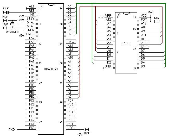
The program stored in the EPROM transmits the internal ROM contents (address range $0140 to $1FFF) through a serial port. The timing critical parts are marked by the number of clock cycles in the comments. Any modification of them should preserve the execution time.
Serial port settings:
![]() 6305y1.zip - EPROM image file
6305y1.zip - EPROM image file
portc   equ     $02
ddrc    equ     $06
ram     equ     $40             ;RAM starting address

; bits of the port C
TXD     equ     0               ;serial output, do not change!

        org     $1F00
reset:  sei
        rsp

; the program is copied to RAM then executed
        clr     x
loop1:  lda     progr,x
        sta     ram,x
        inc     x
        bpl     loop1           ;128 bytes are copied
        jmp     ram

; code copied to RAM
progr:  lda     #$01            ;1<<TXD
        sta     ddrc            ;TXD = output
        sta     portc           ;TXD = high
; delay ca. 500 ms
        clr     x
loop2:  dec     a
        bne     loop2
        dec     x
        bne     loop2

; switch the microprocessor mode
        clr     $1F

; byte loop
loop4:  bclr    TXD,portc       ;start bit
ldacmd: lda     $0140           ;4 cycles, modified operand
        sec                     ;1 cycle, stop bit
; bit loop, required length = 2.4576MHz / 4 / 9600Hz = 64 cycles
loop5:  ldx     #10             ;2 cycles
loop6:  dec     x               ;2 cycles
        bne     loop6           ;3 cycles
        ror     a               ;2 cycles
        rol     portc           ;5 cycles, Carry goes to TXD
        cmp     #0              ;2 cycles, clears Carry
        bne     loop5           ;3 cycles, next bit
; stop bits, number of cycles not critical, but at least 59 from here to loop4
        ldx     #30
loop7:  dec     x
        bne     loop7
; next address
        inc     ldacmd+2+ram-progr
        bne     loop4
        inc     ldacmd+1+ram-progr
        brclr   5,ldacmd+1+ram-progr,loop4
; done
        bra     *

; RESET vector
        org     $1FFE
        db      high reset, low reset