| Index | wersja polska |
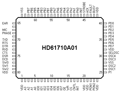
The chip HD61710A01 is the main component of the Casio interfaces MD-100, FA-7, FA-80.
| Pin | Symbol | Function |
|---|---|---|
| 2..5 | A3..A0 | address signals connected to these inputs select the chip registers, the state of the A3 input seems to be ignored |
| 6..13 | IO0..IO7 | bi-directional data bus |
| 14 15 16 | OE WR CS |
bus interface signals |
| 17 | CNTL | reset input, high level = active, low level = normal operation |
| 18 | INT | interrupt request output, active low |
| 22,23 | PON1,PON2 | low level turns the power supply for the internal logic on |
| 25 | P1 | reset output, active high |
| 26,27 | OSC1,OSC2 | ceramic resonator 612kHz, OSC1 is the output from the inverting oscillator amplifier |
| 29,30 | OSC3,OSC4 | quartz crystal resonator 2.4576MHz, OSC4 is the output from the inverting oscillator amplifier |
| 31 | SELOSC | clock source option: high level selects the oscillator OSC1,OSC2 low level selects the oscillator OSC3,OSC4 |
| 33..40 | PD7..PD0 | printer data port |
| 42 43 44 | BUSY FAULT ACK |
printer status port |
| 45 46 | STROBE INIT |
printer control port |
| 47..54 | PA0..PA7 | general purpose input port, function depends on the interface unit: FA-7 - all pins connected to VSS FA-80 - state of the print mode switches MD-100 - data read from the FDD system The calculators PB-1000 and PB-2000C read this port to determine the kind of connected device. Assignment of values: &HFF - no I/O device present &H00 - FA-7 &H55 - MD-100 (value returned immediately after the reset, before any FDD transfer) |
| 55..62 | PB0..PB7 | general purpose output port, function depends on the interface unit: FA-7, FA-80 - pin PB7 controls the cassette motor relay MD-100 - data written to the FDD system |
| 65 67 68 | EAR MIC PHASE |
cassette interface port |
| 70 | TXD | serial port transmit data output |
| 71 72 | RTS DTR |
serial port control signals |
| 73 | RXD | serial port receive data input |
| 74 75 76 | CTS DSR DCD |
serial port status signals |
| 77..79 | SW0..SW2 | baud rate select switches |
| A2 | A1 | A0 | Access | Function |
|---|---|---|---|---|
| 0 | 0 | 0 | Write | serial port control register bit 0 - set when MT, cleared when RS232C bit 1 - set when parity odd, cleared when parity even bit 2 - cleared turns the parity control on bit 3 - set when 7 data bits, cleared when 8 data bits bit 4 - set when 1 stop bit, cleared when 2 stop bits bits 5..7 - baud rate |
| Read | serial port status register bit 0 - set when TX buffer full, cleared after the byte has been transmitted bit 1 - set when RX buffer full, cleared after reading the RX data register 010 bit 2 - state of the CTS input (inverted) bit 3 - state of the DSR input (inverted) bit 4 - state of the DCD input (inverted) bit 5 - receive error flag bits 6..7 - cleared on valid carrier tone from the tape, i.e. when the frequency deviation does not exceed -30% (bit 6) to +100% (bit 7) | |||
| 0 | 0 | 1 | Write | serial port control register bit 0 - transmitter enable bit 1 - receiver enable bit 2 - state of the RTS output (inverted) bit 3 - state of the DTR output (inverted) |
| Read | serial port status register bits 0..2 - receive errors bit 3 - state of the SW0 input bit 4 - state of the SW1 input bit 5 - state of the SW2 input | |||
| 0 | 1 | 0 | Write | serial port control register bit 0 - interrupt request when RX buffer full |
| Read | serial port receive data register | |||
| 0 | 1 | 1 | Write | serial port transmit data register |
| Read | general purpose input port PA | |||
| 1 | 0 | 0 | Write | general purpose output port PB |
| Read | printer status port bit 0 - state of the BUSY input bit 1 - state of the FAULT input bit 2 - set by a pulse on the ACK input, reset by writing logical 1 to bit 2 of register 110 bits 3..7 are expected to be 0 | |||
| 1 | 0 | 1 | Write | printer data port PD |
| 1 | 1 | 0 | Write | printer control port bit 0 - state of the STROBE output bit 1 - state of the INIT output bit 2 - logical 1 resets the ACK latch |
| bits 765 |
baud rate |
|---|---|
| 000 | 9600 |
| 001 | 4800 |
| 010 | 2400 |
| 011 | 1200 |
| 100 | 600 |
| 101 | 300 |
| 110 | 150 |
| 111 | 75 |
Information about those bits, extracted from various ROM disassembly listings, is inconsistent.
If the error flag in register 000 is set, then the contents of register 001 is examined to determine the exact cause:
If the error flag in register 000 is set, then the contents of register 001 is examined:
The error flag in register 000 isn't checked, but a general "read error" is reported when any of bits 0..2 in register 001 is set.