| Index | wersja polska |
On this page only information specific to the PB-2000C is shown. See the PB-1000 hardware page for more general information about the microprocessor and the bus waveforms.
CS0: &H10000..&H17FFF, built-in RAM 32kB
CS1: &H18000..&H1FFFF, built-in RAM extension 32kB and the default address range for the RP-33 module (when pad 4 is open and pad 5 soldered)
CS2: &H28000..&H2FFFF, alternative address range for the RP-33 module (when pad 5 is open and pad 4 soldered)
CS3: &H30000..&H3FFFF, unused
CS4: &H00D90..&H0FFFF, unused
CS5: &H04000..&H05FFF, peripheral port
CS6: &H00C10..&H00C11, gate array (memory configuration registers)
CS7: &H00C00..&H00C0F, gate array (excluded locations), serial, printer and FDD interface
P7..P6 drive the piezo-buzzer
P5 is the reset output for peripherals
P4 controls the FDD power, 0 turns the power on
P3 selects the FDD transfer direction, 1 when writing to the FDD interface, 0 when reading from the FDD interface
P2 is the FDD transfer direction acknowledge input
P1 senses the card presence (low voltage level when a card is inserted)
P0 selects the language version, connected through a jumper either to VSS (English PB-2000C) or to GND (Japanese AI-1000)
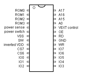
| Pin | Symbol | Function |
|---|---|---|
| 1 | ROM0 | chip select output for the internal ROM with the C interpreter, active low, decodes address range &H00000..&H0FFFF with exclusion of segments decoded by outputs ROM2 and ROM3 |
| 2 | ROM1 | not used, decodes fixed address range &H10000..&H2FFFF |
| 3 | ROM2 | selects the card slot pin 20, decoded address range specified with register &H00C10 |
| 4 | ROM3 | selects the card slot pin 33, decoded address range specified with register &H00C11 |
| 5 | power sense | receives high level from the S8054ALR battery monitor chip when valid supply voltage is present |
| 6 | power switch | receives low voltage level when the power switch is turned on and the card locked |
| 7 | VSS | negative supply voltage |
| 8 | SW | this output drives the microprocessor pin 36, low voltage level turns the system on |
| 9 | inverted VDD | senses the microprocessor pin 33 state through an inverter built with a pnp transistor |
| 10 | CS7 | low level at this input disables the ROM0..ROM3 signals, used to exclude address range &H00C00..&H00C0F occupied by the FA-7/FD-100 interface |
| 11 | CS6 | chip enable input for the configuration registers, receives low level from the CPU for address range &H00C10..&H00C11, low level at this input disables the ROM0..ROM3 signals |
| 12..19 | IO0..IO7 | bi-directional data bus |
| 20 | WR | bus write strobe signal, active low |
| 21 | GND | positive supply voltage |
| 22 | RD | bus read strobe signal, active low |
| 23 | OE | data strobe control signal |
| 24 | VEXT control | low voltage level enables the LCD driver power supply |
| 25..28 | A0, A15..A17 | address bus |
| register bit | enabled combination of address bits | decoded address range |
|---|---|---|
| 0 1 2 3 4 5 6 7 |
A17..A15 = 000 A17..A15 = 001 A17..A15 = 010 A17..A15 = 011 A17..A15 = 100 A17..A15 = 101 A17..A15 = 110 A17..A15 = 111 |
&H00000..&H07FFF &H08000..&H0FFFF &H10000..&H17FFF &H18000..&H1FFFF &H20000..&H27FFF &H28000..&H2FFFF &H30000..&H37FFF &H38000..&H3FFFF |
The actual decoded address range of the first memory segment is limited to &H00C12..&H07FFF. Apart from the excluded memory locations &H00C00..&H00C11, the CPU never puts an address below &H00C00 to the external bus.
Bits 2 and 3 of the configuration register must not be set due to bus conflicts with the RAM in the memory bank 1.
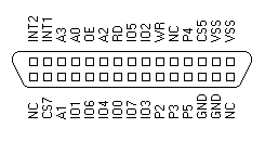
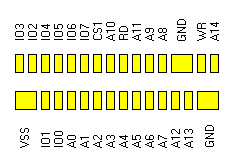
  01 - VSS        16 - IO5        31 - A17
  02 - A12        17 - IO6        32 - GND
  03 - A7         18 - IO7        33 - ROM3
  04 - A6         19 - GND        34 - GND
  05 - A5         20 - ROM2       35 - GND
  06 - A4         21 - A10        36 - NC
  07 - A3         22 - RD         37 - NC
  08 - A2         23 - A11        38 - NC
  09 - A1         24 - A9         39 - NC
  10 - A0         25 - A8         40 - NC
  11 - IO0        26 - A13        41 - NC
  12 - IO1        27 - WR         42 - NC
  13 - IO2        28 - A14        43 - NC
  14 - IO3        29 - A15        44 - P1
  15 - IO4        30 - A16        45 - GND
pin 20 - ROM2 chip enable (gate array pin 3)
pin 33 - ROM3 chip enable (gate array pin 4)
pin 44 - microprocessor port P1, senses the card presence, connected to VSS inside the card
VEXT is the LCD driver supply voltage of ca. -7V
The columns of the keyboard matrix are driven from the 12-bit KO output port, controlled by the IA register. A pressed key makes contact between selected column and row. The rows are sensed by the 12-bit KI input port, accessible through the KY register.
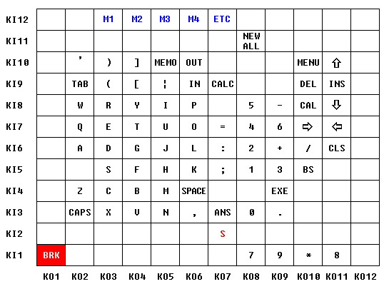
Mapping of the KY register bits to the keyboard rows:
![]()
GND is the positive terminal of the supply voltage, VSS is the negative terminal.
GND is the positive terminal of the supply voltage, VSS is the negative terminal.